InSystemFlasher: Difference between revisions
(→Status) |
m (→Features) |
||
| Line 8: | Line 8: | ||
=Features= | =Features= | ||
* Tester consists of two circuit boards: main and auxiliary board. Main tester board connects to host via USB, and to aux board via ribbon cable. | * Tester consists of two circuit boards: main and auxiliary board. Main tester board connects to host via USB, and to aux board via ribbon cable. | ||
** Smaller boards are easier to build | |||
** Minimize the size of tester to be plugged into mainboard, in case there are obstructions. | |||
** Modular hardware to later accommodate other ROM types besides SPI. | |||
* Optionally, the main tester board can be connected to the reset and ATX power pins of the target mainboard. All common sense voltages (1..5V) are supported. | * Optionally, the main tester board can be connected to the reset and ATX power pins of the target mainboard. All common sense voltages (1..5V) are supported. | ||
* The main tester board has a standard serial port for reading debug output from the target mainbaord. | * The main tester board has a standard serial port for reading debug output from the target mainbaord. | ||
Revision as of 20:20, 27 February 2011
Introduction
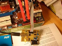
This page describes a tester device, which is capable of programming a BIOS ROM chip while it is connected to a live mainboard. The tester is controlled by a host PC via USB. The purpose of this tester device is to provide a do-it-yourself hardware for testing Coreboot builds. The goal is to support automated builds and tests from version control repository.
The tester is built around the Atmel AT90USB162 microcontroller, which is programmed using avr-gcc and the LUFA library. The host-side software is currently Flashrom.
Features
- Tester consists of two circuit boards: main and auxiliary board. Main tester board connects to host via USB, and to aux board via ribbon cable.
- Smaller boards are easier to build
- Minimize the size of tester to be plugged into mainboard, in case there are obstructions.
- Modular hardware to later accommodate other ROM types besides SPI.
- Optionally, the main tester board can be connected to the reset and ATX power pins of the target mainboard. All common sense voltages (1..5V) are supported.
- The main tester board has a standard serial port for reading debug output from the target mainbaord.
- PCB layout is kept simple, so that it can be built using hobbyist methods, e.g. toner transfer PCB etching. The parts have been chosen so that they should be quite well available and inexpensive.
- Designed using open source tools.
Status
- Currently supports SPI ROMs only.
- Current firmware and flashrom extension do not support serial port or reset/power switch operation.
TODO:
- Flashing speed could be improved. Now reading 1 MByte takes ~70 sec, flash & verify takes ~150 sec.
- Redesign the protocol between microcontroller and host software. (Firmware, host USB driver, flashrom module, and possible other applications)
- Add possibilty to control a relay to switch mains power to test target on and off.
- Add voltage sense lines to detect voltage levels in the test target.
- Extend design to support other ROM types also.
- Integrate to Coreboot automated test system.
Hardware
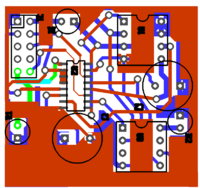
In the images shown are two-sides circuit boards. Red mask shows component-side copper and blue mask shows solder-side copper.
Main PCB
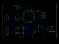
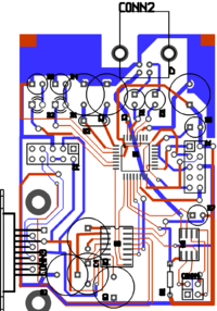
Parts list
- R1,R2: USB line termination resistors. 22 ohm.
- R3,R4: LED current limiters. 270 ohm.
- R5,R6,R7: Pull-ups. 10k ohm.
- C1,C2: Oscillator capacitors. 22 pF.
- U2: Crystal oscillator. 16 MHz.
- C3,C4,C5,C6: Charge pump capacitors. About 100 nF.
- C7: Power bypass. Used 1 microF.
- J1: 2x5 pin header. Pins 1-6 are used to load AVR firmware. Pins 1-6,9,10 connect to aux PCB.
- J2: Alternative connector for RS232.
- CONN4: 2x2 pin header
- CONN2: USB B (device-side) connector.
- CONN3: DB-9 male connector with 90° angle.
- U1: Atmel AT90USB162 in TQFP-32.
- U3: Texas Instruments MAX3232ECDG4 in SOIC-16.
- U4: Texas Instruments SN74CBT3306D Dual FET bus switch in SOIC-8.
- D1,D2: LEDs. Used green and yellow.
Auxiliary PCB
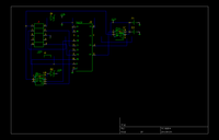
Parts list
- U1: DIP-8 socket for SPI ROM chip.
- U2: SOIC-16 Texas Instruments SN74CBTLV3257D FET Multiplexer
- U3: DIP-8 pin header on the solder-side of the board (plugs to mainboard ROM socket)
- C1,C2: Power bypass capacitors. 100nF worked fine.
- D1,D2: Schottky diodes with low forward voltage drop. Here SD103A-T/R
- R1: Pull-up resistor. 120 kohm was used.
- J1: 2x5 pin header for connecting to tester main PCB. Pins 7 and 8 are not used.
Firmware
The AVR firmware is based on the LUFA library. Version 101122 was used in development.
Host-side software
Downloads
Download sources from Git repository.
TODO: Add URL here.